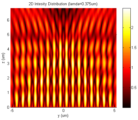
Talbot Lithography is a semiconductor process, which is used for fabrication a sub-micron features in non-contact fashion. This type of lithography uses the light diffraction in the near field (Talbot Effect) for creation a resist image. The example of so called ‘Talbot Carper’ is presented on rigth side image.
Due to high complexity of full fabrication process, which includes optical exposure and chemical development, a software which can simulate the Talbot Lithography will reduce time and cost of prototyping semiconductors devices.
Specification:
- support for an arbitrary mask of two types: amplitude or phase,
- output of Talbot Carpet,
- output of an optical aerial image at specific position and for predefined integration distance,
- calculation of a latent image in photo-resist after exposition ( Dill model ),
- simulation of the development process of the photo-resist ( Notch model ).
Programming skills:
- Matlab
- Optimisation of memory management
- Design User Interface (UI)
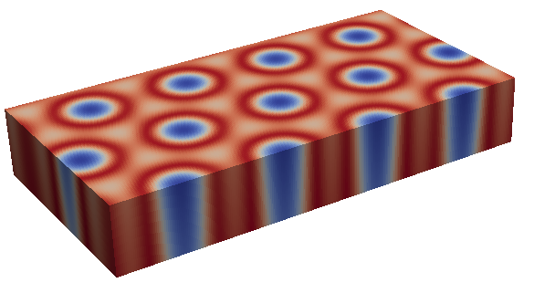
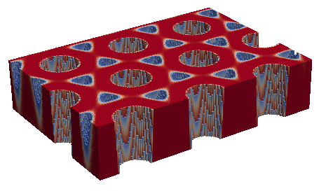
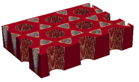
Fig. (Left) Latent image of resist after exposure; (Middle) Final resist representation after short development time; (Right) Final resist representation after long development time.
Papers related to this work:
- E.D. Le Bouldbar, P. J. P. Chausse, S. M. Lis, P. A. Shields, “Displacement Talbot lithography: an alternative technique to fabricate nanostructured metamaterials “, Proc. of SPIE Vol. 10248 102480Q-1 (2017)